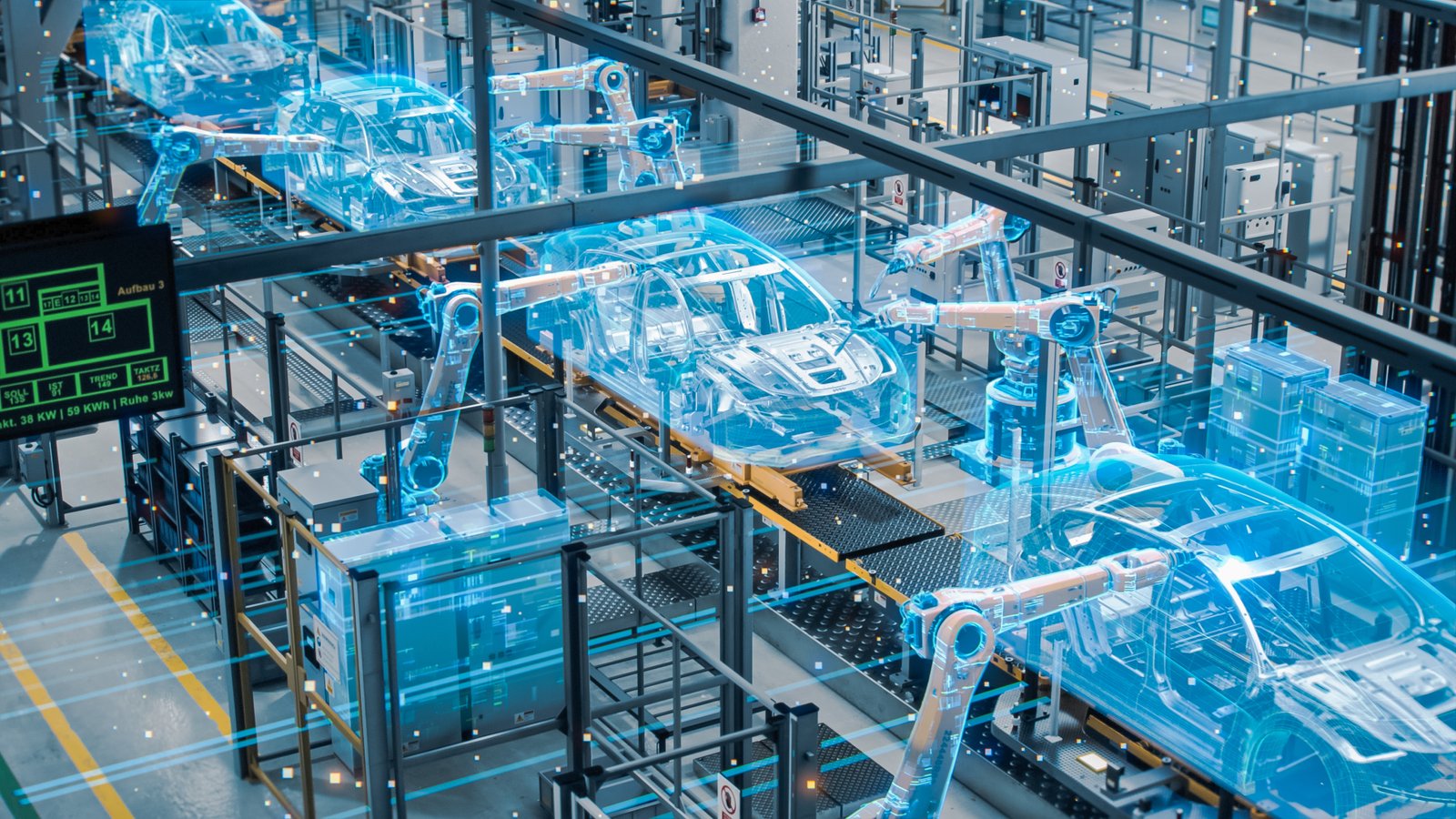
In the contemporary automotive landscape, cars are increasingly perceived as "computers on wheels." The pervasive influence of microcontrollers has transformed every aspect of vehicular functionality, from mundane tasks like window operations to sophisticated calculations optimizing fuel-air mixtures based on real-time torque demands. Yet, this represents just the tip of the iceberg as the automotive industry embraces an era where computing power takes center stage within vehicles.
The Surge of Autonomous Vehicles: L3 Advancements and the Rise of RoboTaxis
As we stand on the brink of the autonomous transportation era, a paradigm shift in computational requirements is reshaping the automotive industry. The advent of automated vehicles demands an extensive array of sensors to scan and interpret the environment, providing the vehicle with the data essential for replicating human driving capabilities. Cutting-edge SAE level 4 robotaxis, equipped with up to 40 individual sensors, underscore the increasing reliance on sensor technologies. This, coupled with the imminent integration of automated technologies across the vehicle market, is propelling the automotive sensors market with a projected 10-year Compound Annual Growth Rate (CAGR) of 13%. However, the efficacy of sensors hinges on high-performance computing (HPC), which processes real-time data outputs, constructs a 3D rendering of the environment, and informs the vehicle's programmed driving policy.
High-performance computing (HPC) plays a pivotal role in handling the deluge of data generated by various sensors, addressing critical challenges such as sensor fusion and object classification. The debate surrounding the sequencing of these processes persists. Some advocate for early fusion, where all sensor data converges into a 3D representation of the scene, allowing an AI algorithm within the vehicle's HPC unit to identify and label each detected object. Conversely, others favor generating an object list from individual sensors before consolidating the results. This approach enables cross-referencing detections from different sensors to ensure agreement but introduces complexities in managing discrepancies across the various sensor-generated object lists.

The Heart of Autonomous Vehicles: The Autonomous Computing SOC
In the realm of autonomous driving, the brain powering the vehicle's decision-making processes is encapsulated in the Autonomous Computing System on Chip (SOC). Whether employing late fusion or early fusion, the High-Performance Computing (HPC) unit within the SOC undertakes extensive data processing, including image processing and the execution of artificial intelligence algorithms for tasks like image classification and driving policy formulation.
The key components orchestrating these intricate tasks are Graphics Processing Units (GPUs), Computational Processors (CPUs), and Random-Access Memory (RAM). Traditionally discrete, these components have evolved to be integrated onto a single chip, known as an SOC or system on a chip. This integration streamlines the exchange of data between components, minimizing latency, reducing noise interference, and maximizing bandwidth. The SOC's role is all-encompassing, from processing data acquired through autonomous driving sensors to identifying and classifying detected objects, culminating in generating steering, throttle, and brake commands in alignment with the driving policy.
Central to the SOC's efficiency are GPUs, playing a pivotal role in image processing and executing AI algorithms, particularly in deep learning and Neural Networks. Notably, Nvidia has emerged as a frontrunner in the autonomous vehicles sector, leveraging its expertise in GPU development for graphical computing applications. Platforms like Xavier and Orin from Nvidia have become staples in the realm of autonomous vehicle computational processing.
Mobileye, with its inception in 1999, has been a trailblazer in the industry, drawing attention and prompting an acquisition by Intel. Having since regained its public status, Mobileye has found widespread application in consumer vehicles, powering Advanced Driver Assistance Systems (ADAS) applications.
Both Nvidia and Mobileye have made substantial strides in enhancing computational power, transitioning from handling a few Terra Operations Per Second (TOPS) to now dealing with hundreds of TOPS, with an eye on reaching thousands of TOPS. This progress is largely fueled by the adoption of increasingly smaller node sizes from leading foundries such as TSMC and Samsung, marking a continuous pursuit of technological advancements in chip manufacturing.

Growing semiconductor technologies
In recent years, Market has seen Mobileye, Nivida, and others move from 28nm in 2018 to 7nm FinFET solutions and lower in 2021. However, the foundries are now producing sub-5nm technologies and heading toward sub-1nm technologies in the future. Each time the node technology halves, the computation power increases by a factor of 10. But chasing smaller and smaller node sizes will get more and more expensive. A single 300mm wafer of TSMCs 3nm technology costs in the region of US$20,000, and that price will continue to grow as sub-3mn technologies are demanded in a variety of industries, from normal computing applications such as phones, laptops and PCs, to the new demand coming from the automotive sector.
As such, automotive HPC developers need to think about how they can optimize existing technologies to get the most performance. One approach that IDTechEx is seeing is an increasedfocus on artificial intelligence (AI), neural networks (NN), and deep learning (DL) accelerators. These use new data AI-enhanced data processing strategies, reducing the reliance on classical approaches found in the GPU. This can boost the performance of the chip very cheaply, requiring less investment in smaller node technologies and even producing an overall efficiency benefit. IDTechEx is seeing AI becoming more common in SOC block diagrams from leading tier 2s like Mobileye and Renesas. But one particularly interesting prospect is Recogni. Recogni is a start-up that has developed an AI accelerator for autonomous driving SOC applications that promises game-changing computational power and efficiencies.
Even with reducing node sizes and imaginative AI solutions, the larger computer chip industry is still seeing a slowing in the pace of development. Moore's law says that computational power should double every two years, a decades-old empirical formula that has held strong until recently. Some are saying that Moore's law is beginning to slow as the industry faces increasingly difficult technological challenges to achieve smaller and smaller incremental gains. Others say Moore's law is dead.
A prominent solution to deal with the slowdown of Moore's Law and the substantial increase in the manufacturing cost of monolithic integrated circuits (ICs) is the concept of "chiplets." The core concept of chiplets involves deconstructing a monolithic IC into distinct functional blocks, transforming these blocks into separate chiplets, and subsequently reassembling them at the packaging level. The ultimate goal of a chiplet-based processor is to maintain or enhance performance while reducing the overall production expenses compared to traditional monolithic ICs. The efficacy of chiplet design heavily relies on packaging techniques, particularly those employed to interconnect multiple chiplets, as they significantly impact the overall system performance. These advanced semiconductor packaging technologies, encompassing approaches like 2.5D IC, 3D IC, and high-density fan-out wafer-level packaging, are collectively referred to as "advanced semiconductor packaging." They facilitate the convergence of multiple chiplets, often produced at different process nodes, onto a single substrate. This convergence is made possible by the utilization of compact bump sizes, thereby enabling heightened interconnect densities and superior integration capabilities.
Looking at the current landscape of advanced semiconductor packaging technologies in the industry, let's take the server CPU sector as an illustrative example. While most contemporary server CPUs are built around monolithic System-on-Chip (SoC) designs, notable developments have emerged. In 2021, Intel announced its forthcoming server CPU, Sapphire Rapids, which will adopt a novel approach. This next-gen CPU will be constructed as a four-chip module interconnected via Intel's Embedded Multi-die Interconnect Bridge (EMIB), representing a 2.5D advanced semiconductor packaging solution.
Concurrently, AMD has embraced the power of 3D advanced semiconductor packaging techniques to enhance server CPU performance. In the case of its latest server CPU, Milan-X (released in March 2022), AMD employs a 3D packaging strategy that involves stacking a cache die directly atop the processor. This innovation results in a remarkable >200x interconnect density boost compared to conventional 2D packaging, according to AMD's claims. These developments are not limited to CPUs alone; the data center domain has also witnessed the integration of advanced semiconductor packaging technologies for other components, such as accelerators. NVIDIA, a key player, has been utilizing TSMC's 2.5D packaging technology known as Chip on Wafer on Substrate (CoWoS) for its high-end GPU accelerators since 2016.
This surge of adoption, exemplified by both Intel and AMD in their cutting-edge products, points to a widening utilization of advanced semiconductor packaging technologies across the industry. The trend spans beyond server CPUs, encompassing a variety of data center components. As the industry landscape evolves, these innovative packaging methodologies are poised to play a pivotal role in enhancing performance, integration, and efficiency.